Every modern convenience—from the smartphone in your pocket and the infotainment system in your car to the massive data centers powering the global economy—relies on a microscopic marvel: the semiconductor. For decades, the global supply chain that births these chips operated in the background, a silent engine of industrial progress. That changed in 2021, when a perfect storm of pandemic-induced demand and logistics bottlenecks shuttered auto plants and stalled electronics production, forcing the word "semiconductor" into the daily lexicon of the average consumer.
For professionals in international trade, logistics, and manufacturing, the era of treating chips as a "black box" commodity is over. Understanding the intricate, multi-continental journey of a single semiconductor is no longer a niche interest; it is a fundamental requirement for risk management and operational survival in the 21st century.
The Anatomy of a Chip: A Chronological Journey
The lifecycle of a semiconductor is perhaps the most complex manufacturing process in human history. A single chip may cross a dozen international borders before it is finally soldered onto a printed circuit board.
Phase 1: From Earth to Element
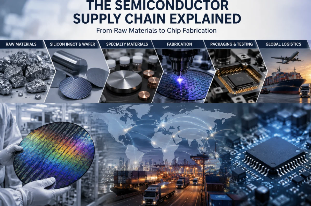
It begins with sand—but not the variety found on a beach. Semiconductor manufacturing requires ultra-pure quartz sand with silicon dioxide levels exceeding 99%. This raw material undergoes a rigorous refining process to become metallurgical-grade silicon, and eventually, electronic-grade polysilicon. This stage is notoriously capital-intensive, concentrated among a small number of global producers. A localized disruption at a single milling plant can ripple through the entire worldwide industry.
Phase 2: The Wafer Foundation
Once refined, the polysilicon is melted and grown into a single-crystal ingot using the Czochralski method. This ingot is sliced into wafer-thin discs, polished to a mirror finish. These wafers (typically 200mm or 300mm in diameter) serve as the platform for all subsequent circuitry. Because wafer production is concentrated among a handful of specialized firms, the market possesses minimal redundancy. When a major provider faces an outage, the global semiconductor market feels the shockwaves almost immediately.
Phase 3: The Overlooked Layer – Specialty Materials
Between the wafer and the finished chip lies a "hidden" layer of supply: specialty chemicals, photoresists, and high-precision metals. Of particular note are sputtering targets—precision-engineered discs of metals like copper, tantalum, or titanium. These targets are used to apply ultra-thin films that form the electrical connections within the chip. Because the performance of the chip is tethered to the purity of these targets, the manufacturers behind them are critical chokepoints in the global chain.
Phase 4: The Fab – Where Complexity Lives
The "fab" (fabrication facility) is the crown jewel of the process. Within these multi-billion-dollar environments, wafers undergo hundreds of nanometer-scale steps:
- Lithography: Using light to project complex patterns onto the wafer.
- Etching: Sculpting these patterns by stripping away material.
- Deposition: Applying layers, such as metal films via sputtering.
- Doping: Introducing controlled impurities to manipulate silicon’s electrical conductivity.
Phase 5: Packaging, Testing, and Final Logistics
Post-fabrication, the wafer is diced into individual chips, which are then packaged—a process that provides the physical protection and electrical contacts necessary for board integration. Traditionally centered in Southeast Asia (Malaysia, Vietnam, Philippines), this stage is followed by rigorous testing. A single defective chip in an automotive braking system or medical device can result in catastrophic costs, making testing a mandatory, non-negotiable stage of the chain.
Supporting Data: Why Concentration Equals Risk
The semiconductor supply chain is defined by an extreme lack of geographic and corporate diversity.
- Geographic Bottlenecks: Taiwan produces the vast majority of the world’s most advanced semiconductors. This centralization creates a geopolitical "single point of failure" that remains a primary concern for global security and trade analysts.
- Rigidity of Capacity: Building a state-of-the-art fab requires a lead time of three to five years and investments reaching $10 billion to $20 billion. Consequently, the industry cannot pivot to meet sudden demand surges—a structural reality that transformed the pandemic’s temporary supply chain hiccup into a multi-year global shortage.
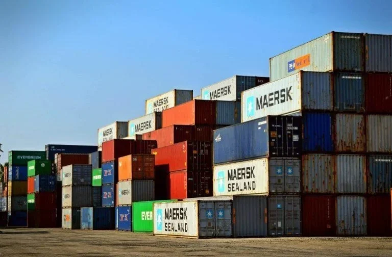
- Logistical Complexity: Because the value of a chip is immense relative to its weight, finished products move via air freight, while the heavy equipment and raw materials required to make them move by sea. This dichotomy exposes the chain to both port congestion and the volatile costs of air logistics.
Official Responses and Strategic Shifts
In response to the 2021 crisis, governments worldwide have pivoted from a "just-in-time" philosophy to a "just-in-case" strategy.
The U.S. CHIPS and Science Act, along with similar legislative initiatives in the European Union, India, and Japan, signals a return to industrial policy. Governments are now providing massive subsidies to lure leading-edge fabrication facilities back to domestic soil. The goal is to move from a highly centralized, "fragile" model to a regionalized, "resilient" model.
However, industry leaders warn that this transition is fraught with challenges. As noted by the Washington Post and various trade journals, the lack of a specialized workforce and the reliance on a global web of chemical suppliers means that "onshoring" is not a simple flip of a switch. It is a decadal commitment to rebuilding an ecosystem that was outsourced over the previous thirty years.
Implications for Global Trade Professionals
The semiconductor saga offers a cautionary tale for any professional involved in procurement, supply chain management, or international trade.
1. The Death of the "Black Box"
Companies can no longer afford to ignore their tier-two and tier-three suppliers. If a business relies on a component that contains a chip, they are indirectly reliant on the availability of sputtering targets, photoresists, and the political stability of the Taiwan Strait. Visibility must extend to the very origin of raw materials.
2. The Cost of Redundancy
For years, efficiency was the singular goal of supply chain management. Today, the metric has shifted toward resilience. This means holding higher levels of strategic inventory and paying a premium for regional suppliers, even when global alternatives are cheaper.
3. Navigating Export Controls
The rise of geopolitical friction has redefined sourcing. Trade regulations, export controls, and tariffs on chip-making equipment have forced a bifurcation of the global market. Trade professionals must now navigate a complex map of regulatory compliance that changes by the month, requiring a new level of legal and geopolitical literacy.
Conclusion
The path from a grain of sand to a high-performance microprocessor is a testament to human ingenuity, yet it remains one of the most brittle structures in modern commerce. The semiconductor industry has revealed that extreme specialization, while efficient in times of peace and stability, creates immense fragility when the world is tested by crisis.
For the modern trade professional, the lesson is clear: the semiconductor supply chain is not merely a logistical problem to be solved, but a strategic environment to be navigated. As companies move to diversify their supplier bases and governments invest in domestic capacity, the ability to map, monitor, and mitigate risks within this intricate web will be the defining competitive advantage of the next decade. Understanding the journey of the chip is no longer a matter of idle curiosity—it is the bedrock of business continuity in an increasingly interconnected, yet volatile, global economy.
About the Author